


As the name suggests, a high speed printed circuit board design provides the transmission of signals at high speeds. In other words, a device with a high speed design PCB can transfer data at a very high rate. This capability opens up a lot of opportunities for engineers and manufacturers, helping them create the most advanced electronic solutions.
With that, it raises certain difficulties at the development stage that mostly relate to the integrity of signals propagating across the board. You can relieve the integrity issues by choosing the right PCB material, but you can still face some serious challenges, including:
- electromagnetic interference (EMI);
- signal propagation delays;
- crosstalk;
- signal degradation.
The generally accepted PCB design standards will not always work here. There are special high speed PCB layout techniques that can simplify the design process and help you avoid potential issues. We’ll talk about these techniques later in the article, but first of all, let’s point out the main features typical of a high speed PCB.
You can identify a high speed PCB design by certain characteristics. So, the design is high speed if:
- it uses HDMI, Ethernet, SATA, PCI Express, USB, Thunderbolt, or other high speed interfaces for the fast data transfer;
- the circuit consists of several sub-circuits connected to each other through high speed interfaces (LVDS, DSI, CSI, SDIO, DDR3, etc.);
- the time of signal propagation over the track is at least ⅓ of the signal rise time;
- the digital signal frequency is of 50MHz and over;
- the size of the printed circuit board is very small, and the location of the components becomes a real challenge (especially when you come across a high speed interface layout).
To sum up, high speed PCB design is applied to devices with PCBs working at high frequencies with the use of high speed interfaces. With that, the amount of data and speed of its transfer mean the world.
As in every engineering process, there are certain rules and directions on how to design a high speed PCB schematic and layout. Let us consider the key points and challenges which may arise at the same time.
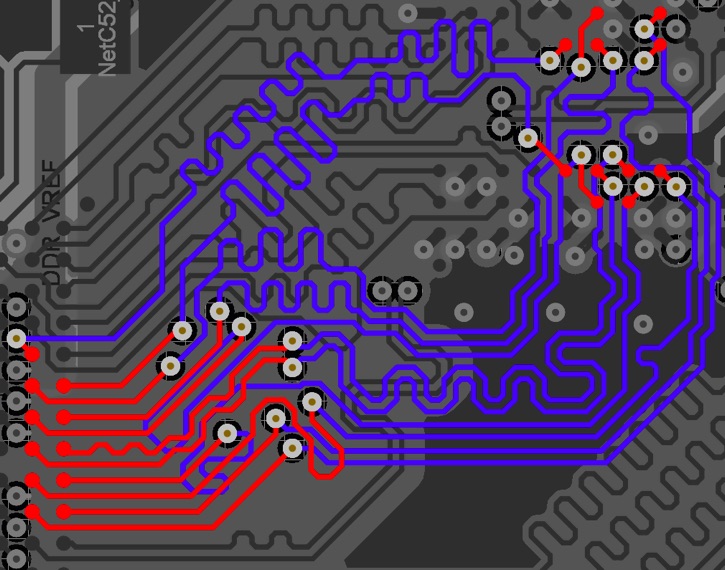
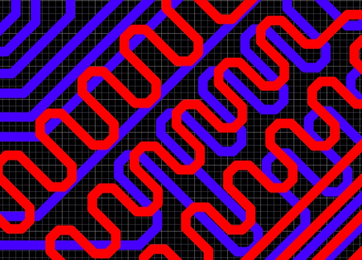
When you use a high speed interface, you need to tune the length of the traces to synchronize signal propagation through data lines. If it is not synchronized, the interface could fail at the maximum frequency or will not work at all. That is why tuning the trace length is a critical aspect in a high speed design.
The higher the interface frequency, the higher the requirements of the length matching. As you know, there are two types of interfaces in PCB design and length tuning will be different for each of them. For a parallel interface, we tune only the lengths of the traces. The main challenge is that there are many traces with a lack of space for length tuning. For a serial interface, we unite signals into several differential pairs.
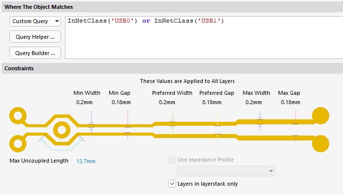
Length matching rules for differential pairs are more complicated. All traces should have the same length with a tolerance of X mm. With that, the length of the traces should be equal in each pair with a tolerance of Y mm, given that Y < X.
Aligning of the traces’ lengths leads to the loss of the distance equality between the tracks of a differential pair. You should make sure that the length of such equality-loss regions is not more than the maximum uncoupled length.
For extremely high speed interfaces, it is important to remember about the interconnecting delays inside CPUs, FPGAs, etc. Bear these delays in mind when you tune the tracks’ length.
Modern CADs have built-in tools for trace length tuning. Before you start using such tools, you should define aligning rules for each of the interfaces. It is important to know which particular rules and limitations you should define.
When you make a PCB layout or a high speed PCB layout, you should observe single-ended impedance Zo as well as differential impedance Zdiff.
As a refresher: single-ended impedance is the impedance of single tracks that are not united into differential pairs. Differential impedance is the impedance between a pair of coupled tracks.
There are typical impedance values for each interface both parallel and serial.
There are also other types of impedance:
- Odd Mode Zoo (half the value of the differential impedance)
- Common Zcm (into a pair of lines with identical signals)
- Even mode Zoe (twice the common mode value)
These impedances are quite rare though you shouldn’t forget about them. The wrong single-ended or differential impedance will lead to the signal reflections inside the track. This will result in the loss of signal quality, decrease of working frequency and generation of unwanted EMI.
That is why adherence to the right impedances is one of the most important rules of the high speed PCB design.

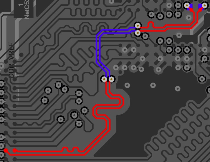
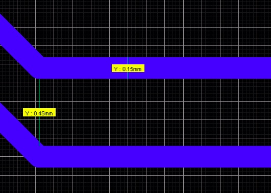
You can hardly ever meet straight tracks from the sources to the receiver on boards. Especially in the context of high speed interfaces where you have to bend the tracks while tuning their lengths.
Ideally, tracks should have rounded, smooth corners without sharp bends. However, you need plenty of time to achieve this.
What makes such a design even more time-consuming is that you redraw each track several times during the layout optimization.
The worst case is to bend tracks at 90-degree angles. The thing is that the width of the track changes drastically at the bends. As a result, impedance changes in these places and reflections appear in the track. In the case of differential pairs, this also leads to a higher value of uncoupled length.
For this reason, the best option is to bend tracks at an angle of 45 degrees.
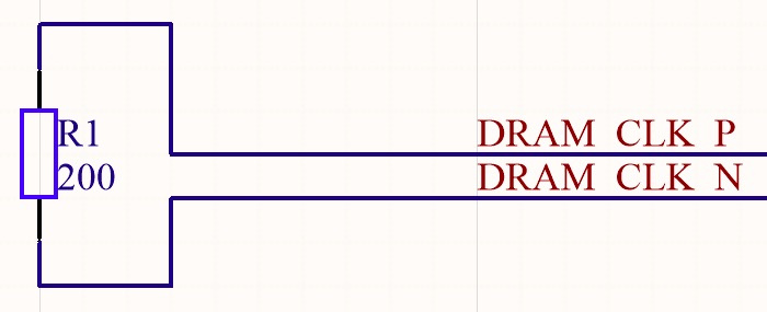
Today the most common type of termination is parallel termination. The idea is to place a resistor between the tracks of a differential pair at the end of the line, as close to the receiver as possible.
Termination makes it possible to effectively get rid of signal reflections in the tracks, therefore, upgrading the quality of data transfer. In the case of differential pairs, resistor value should be equal or a little more than Zdiff.
The low value of the resistor will cause over-termination which will adversely impact the signal quality.
Some ICs have termination resistors inside. In this case, you do not need external resistors because they will cause over-termination. That’s why it is important to learn datasheets and hardware design guides for all ICs you use.
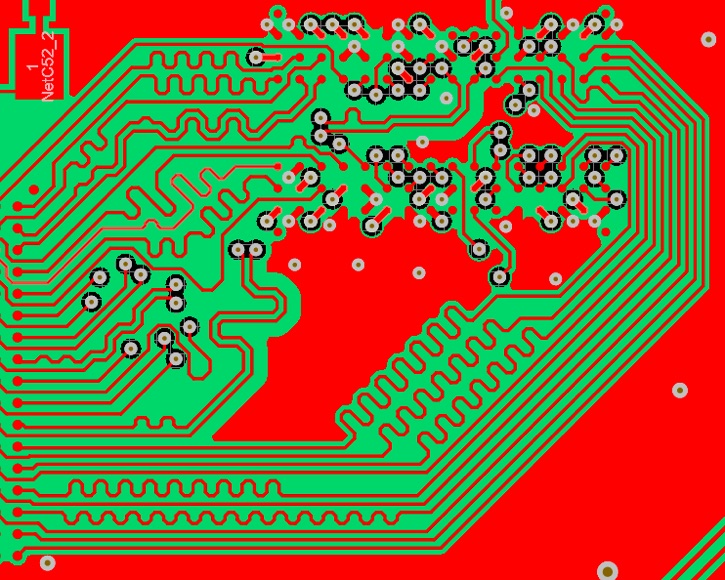
In most cases, you cannot trace high speed interfaces on one layer. Thus you need to move traces to the other layers with the help of vias. Vias are electroplated holes through which traces can connect with each other on different board layers.
GND polygons potential on different layers should be the same near signal vias. That’s why you should place GND vias as close to them as possible. Such GND vias are called stitching vias. This approach allows keeping the same GND reference all along the high speed trace.
However, you should be careful with using vias for high speed signal routing. Thus, densely populated vias can lead to high current density and consequently overheating. When placing vias, make sure there is enough space between them.
The improper design of vias can cause impedance discontinuities. To avoid this, all vias should have an appropriate diameter either on the board layout or on the manufactured PCB.
Components’ placement is an important point in the high speed PCB layout rules. Before you begin, try to map out the location of the components on your board.
For example, you can sort out the components according to their functionality. If they take part in one and the same process or perform similar functions, you should locate them close to each other.
Analog components (if there are any on the board) should have their own GND polygon. In addition, you should place them separately from digital components and traces to avoid EMI.
Before placing the high speed components, remember that the traces are not very long. So make sure you leave enough space for the length tuning. There is no point in placing such components very close to the interference sources, such as switching power converters.
Moreover, you shouldn`t place components relating to high speed interfaces too close to the edge of the board. Such placement has a negative impact on signal quality. It’s better to move such components to the center of the board, leaving the connectors on the edge.
The components’ location becomes a real challenge when a PCB is of a very small size. Following the location rules for high speed design, we placed the components in the most accurate manner on a small PCB for a custom IP camera.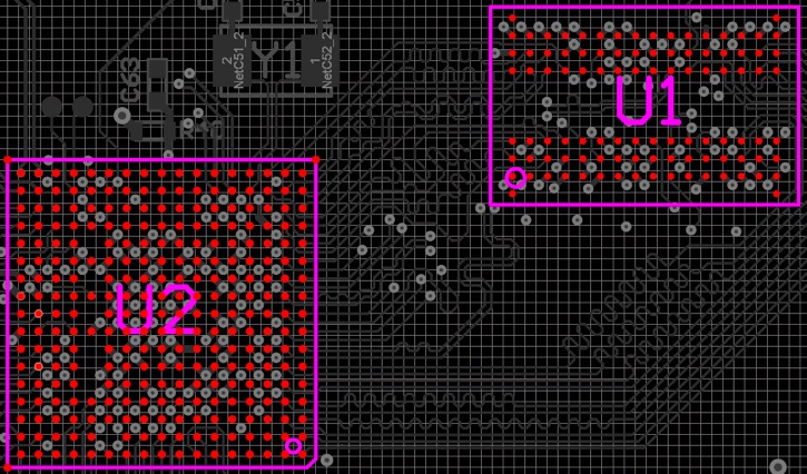
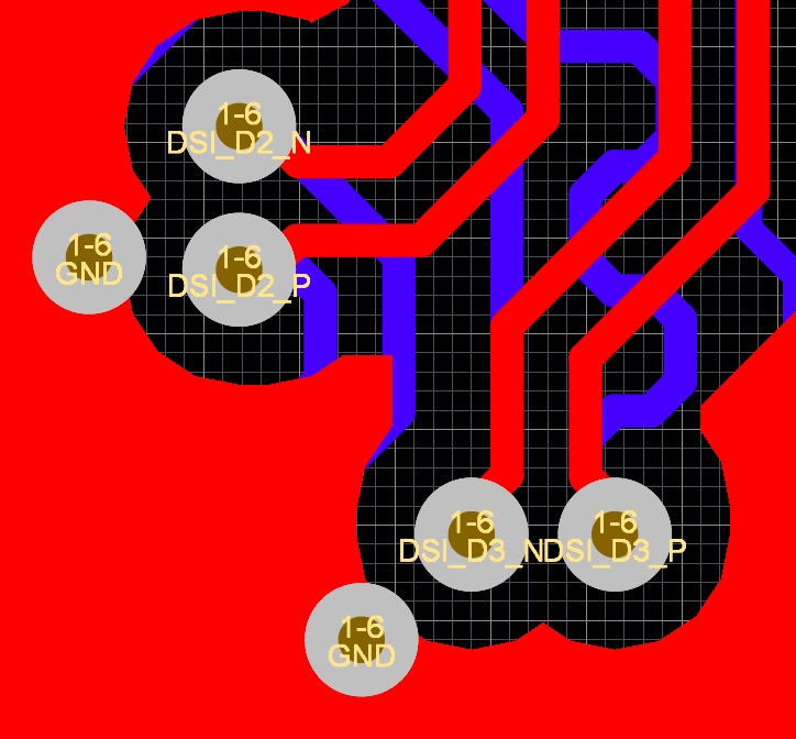
You should route tracks of high speed interfaces over a solid GND plane.
We do not recommend you route tracks over cutouts in polygons or over polygon-splits. Otherwise, you will get extra EMI, signal propagation delays, integrity violation, generation of interference and finally, degradation of the signal quality.
If the tracks happen to cross polygon-splits, it is necessary to place ceramic stitching capacitors at the place of polygons splitting. This will minimize the negative impact on the signal.
Crosstalk is a phenomenon that takes place when a signal transmitted over one communication track raises an unwanted effect in the other tracks. The effect shows as a change in signal and in most cases, the tracks are neighboring.
Crosstalk depends on the length of the section where the tracks run parallel with each other. The longer the section’s length, the higher the crosstalk.
To minimize crosstalk, it is necessary to make the distance between the tracks at least three times longer than the track’s width (3W rule).
To minimize crosstalk between differential pairs, the distance between the differential pairs should be at least five times longer than the track’s width (5W rule). Keep the same distance between differential pairs and any other tracks along the full length of the differential pair.
If a differential pair serves to transmit a periodic signal, e.g. clocking, we recommend you increase the distance from this differential pair to the other differential pairs or any other tracks up to 8-10W.
Pay special attention to the tracks of asynchronous signals (enable, interrupt, reset, etc.). You should make the distance between these tracks and tracks with high speed signals as long as possible.
Sometimes we use two neighboring layers in a multilayer printed circuit board to route signals. Doing this, remember to route the tracks on one layer perpendicular to the tracks on the second layer. Thus you will avoid parallelism of the tracks and minimize crosstalk between them.
We have mentioned the basic high speed PCB board design rules but not all of them. This is a wide area of an even much wider area called PCB design.
In its turn, PCB design is a part of such a vast and multistage domain as embedded hardware development. It includes, for instance, preparation for production and selection of components. At these stages, you should consider bazillion nuances such as the device production time and the scheduled time for discontinued components, etc.


%20Design%20Guidelines%20–%20PCB%20HERO)