


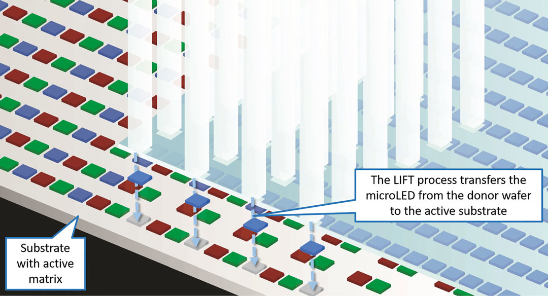
In the Laser-Induced Forward Transfer (LIFT) process, the laser is used to selectively transfer material, such as microLED chips, from a donor substrate to a target substrate.
(Credit: 3D-Micromac)
MicroLEDs have the potential to revolutionize the display industry, promising a variety of advantages such as superior viewing angle, high dynamic range with perfect black luminance and high brightness, wide color gamut, fast refresh rates, long lifetime, and low power consumption. However, the microLED fabrication process is vastly more complex than LCD and OLED manufacturing, and faces several technical challenges that must be overcome before microLEDs can be readily available in the mass market.
Among these challenges is detaching and transferring the processed microLED chips from the donor or growth (e.g., sapphire) substrate to an intermediate substrate for subsequent testing, allowing the expensive growth substrate to be repurposed for future use. Another challenge is to quickly and precisely transfer the chips to the final glass backplane, which for a typical 4K display involving tens of millions of microLED chips could take hundreds of hours using traditional pick-and-place transfer methods. Technologies are also needed that can detect and repair/replace defective microLEDs during the manufacturing process, since a pixel yield rate of 99.9999% is required to produce a full-HD desktop display.
3D-Micromac AG (Chemnitz, Germany), which develops laser micromachining and roll-to-roll laser systems, has introduced its microCETI laser micromachining platform that supports all laser processes in microLED display manufacturing with the high throughput and precision, and low cost of ownership, needed for volume production requirements. This platform is available in three different configurations:
- LIFT: unique laser transfer process for nearly every microLED material and shape
- LLO: on-the-fly laser lift-off suitable for customer related microLED material
- REPAIR: Single-die-repair process at every step of the microLED production
The microCETI platform features a high-precision UV-wavelength laser with high repetition rate and an advanced positioning system for three stages (donor stage, substrate stage and mask stage) and up to 16 axes to transfer every microLED with sub-two-micron positioning accuracy and nanometer-scale repeatability. microCETI supports donor wafer sizes ranging from 50 mm (2 in.) up to 200 mm (8 in.) as well as intermediate/transfer wafers and backplane substrates up to 350 × 350 mm. In addition to microLEDs, the microCETI platform is also suitable for standard LED and miniLED processing.
3D-Micromac is currently accepting orders for the microCETI platform.
Source: 3D-Micromac press release


