


The University of Nottingham has cracked the conundrum of how to use inks to 3-D-print novel electronic devices with useful properties, such as an ability to convert light into electricity.
The study shows that it is possible to jet inks, containing tiny flakes of 2-D materials such as graphene, to build up and mesh together the different layers of these complex, customised structures.
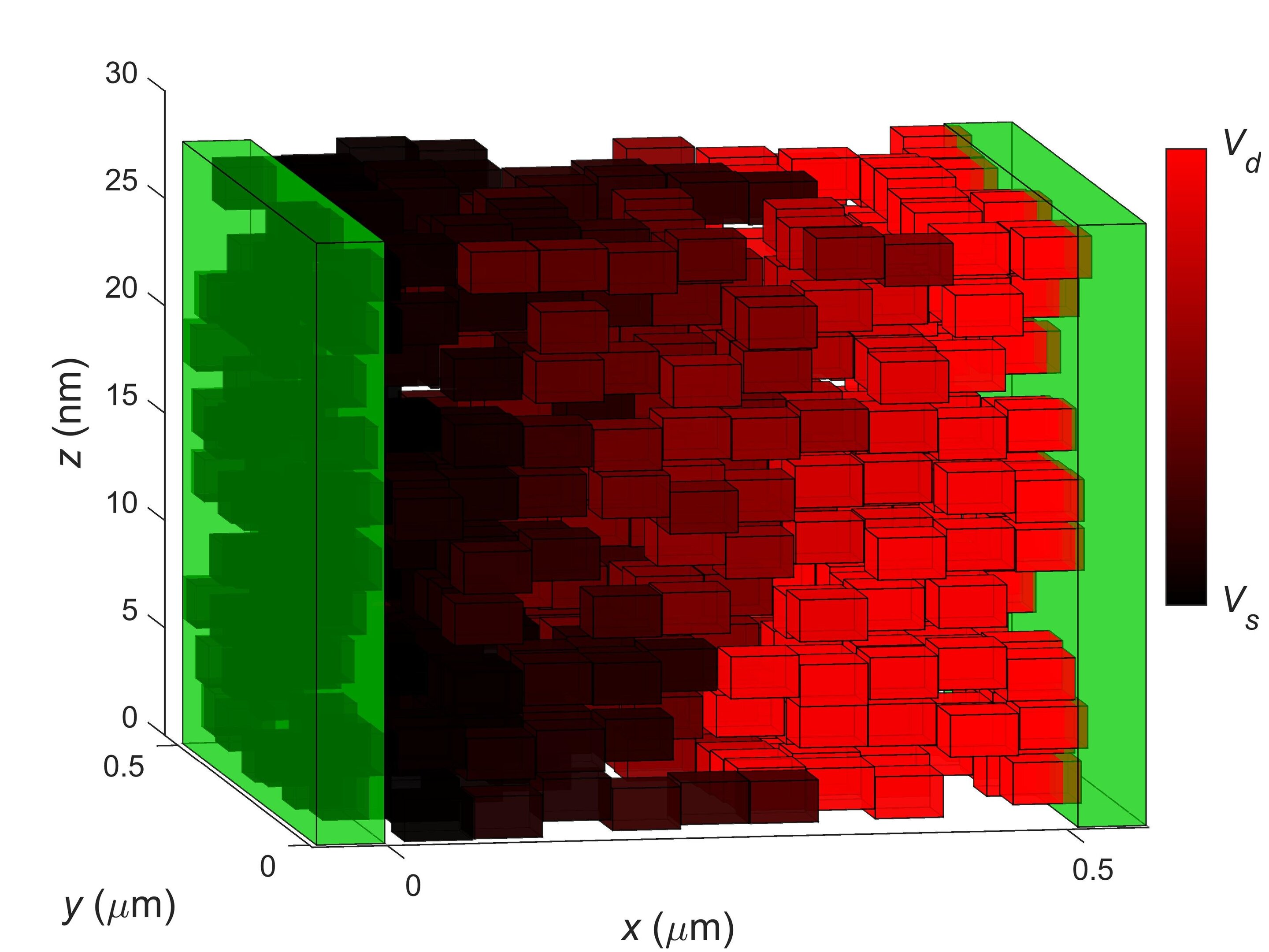
Using quantum mechanical modelling, the researchers also pinpointed how electrons move through the 2-D material layers, to completely understand how the ground-breaking devices can be modified in future.
Paper co-author, Professor Mark Fromhold, Head of the School of Physics and Astronomy said, “By linking together fundamental concepts in quantum physics with state-of-the art-engineering, we have shown how complex devices for controlling electricity and light can be made by printing layers of material that are just a few atoms thick but centimetres across.
“According to the laws of quantum mechanics, in which the electrons act as waves rather than particles, we found electrons in 2-D materials travel along complex trajectories between multiple flakes. It appears as if the electrons hop from one flake to another like a frog hopping between overlapping lily pads on the surface of a pond.”
The study, ‘Inter-Flake Quantum Transport of Electrons and Holes in Inkjet-Printed Graphene Devices’, has been published in the peer-reviewed journal Advanced Functional Materials.
Often described as a ‘super material’, graphene was first created in 2004. It exhibits many unique properties including being stronger than steel, highly flexible and the best conductor of electricity ever made.
Two-dimensional materials like graphene are usually made by sequentially exfoliating a single layer of carbon atoms—arranged in a flat sheet—which are then used to produce bespoke structures.

However, producing layers and combining them to make complex, sandwich-like materials has been difficult and usually required painstaking deposition of the layers one at a time and by hand.
Since its discovery, there has been an exponential growth in the number of patents involving graphene. However, in order to fully exploit its potential, scalable manufacturing techniques need to be developed.
The new paper shows that additive manufacturing—more commonly known as 3-D printing—using inks, in which tiny flakes of graphene (a few billionths of a metre across) are suspended, provides a promising solution.
By combining advanced manufacturing techniques to make devices along with sophisticated ways of measuring their properties and quantum wave modelling the team worked out exactly how inkjet-printed graphene can successfully replace single layer graphene as a contact material for 2-D metal semiconductors.
Co-author, Dr. Lyudmila Turyanska from the Centre for Additive Manufacturing, said, “While 2-D layers and devices have been 3-D printed before, this is the first time anyone has identified how electrons move through them and demonstrated potential uses for the combined, printed layers. Our results could lead to diverse applications for inkjet-printed graphene-polymer composites and a range of other 2-D materials. The findings could be employed to make a new generation of functional optoelectronic devices; for example, large and efficient solar cells; wearable, flexible electronics that are powered by sunlight or the motion of the wearer; perhaps even printed computers.”
The study was carried out by engineers at the Centre for Additive Manufacturing and physicists at the School of Physics and Astronomy with a common interest in quantum technologies, under the £5.85m EPSRC-funded Programme Grant, Enabling Next Generation Additive Manufacturing.
The researchers used a wide range of characterisation techniques—including micro-Raman spectroscopy (laser scanning), thermal gravity analysis, a novel 3-D orbiSIMS instrument and electrical measurements—to provide detailed structural and functional understanding of inkjet-printed graphene polymers, and the effects of heat treating (annealing) on performance.
The next steps for the research are to better control the deposition of the flakes by using polymers to influence the way they arrange and align and trying different inks with a range of flake sizes. The researchers also hope to develop more sophisticated computer simulations of the materials and the way they work together, developing ways of mass-manufacturing they devices they prototype.
News story: New study reveals unexpected softness of bilayer graphene
Feiran Wang et al, Inter‐Flake Quantum Transport of Electrons and Holes in Inkjet‐Printed Graphene Devices, Advanced Functional Materials (2020). DOI: 10.1002/adfm.202007478
Citation:
3-D print experts discover how to make tomorrow’s technology using ink-jet printed graphene (2020, November 4)
retrieved 4 November 2020
from https://phys.org/news/2020-11-d-experts-tomorrow-technology-ink-jet.html
This document is subject to copyright. Apart from any fair dealing for the purpose of private study or research, no
part may be reproduced without the written permission. The content is provided for information purposes only.


