


Abstract
Monolithic strong magnetic induction at the mtesla to tesla level provides essential functionalities to physical, chemical, and medical systems. Current design options are constrained by existing capabilities in three-dimensional (3D) structure construction, current handling, and magnetic material integration. We report here geometric transformation of large-area and relatively thick (~100 to 250 nm) 2D nanomembranes into multiturn 3D air-core microtubes by a vapor-phase self-rolled-up membrane (S-RuM) nanotechnology, combined with postrolling integration of ferrofluid magnetic materials by capillary force. Hundreds of S-RuM power inductors on sapphire are designed and tested, with maximum operating frequency exceeding 500 MHz. An inductance of 1.24 μH at 10 kHz has been achieved for a single microtube inductor, with corresponding areal and volumetric inductance densities of 3 μH/mm2 and 23 μH/mm3, respectively. The simulated intensity of the magnetic induction reaches tens of mtesla in fabricated devices at 10 MHz.
INTRODUCTION
Electrically controlled generation of strong magnetic induction at room temperature is a topic of broad interest in a wide range of science and engineering applications, including magnetic resonance imaging, DNA analyses, biological behavior, and power electronics, among others (1–5). Many such magnetic induction systems use designs following Faraday’s law to exploit similar strategies for realizing large coil densities, integrating high-permeability material, and maximizing current handling ability (6–12). Although a variety of technique innovations are capable of realizing specific structures in certain classes of materials on the macroscale so as to attain the desired performance, micro- and nanoscale fabrication techniques relying on advanced nanotechnologies have the potential to provide an extremely promising platform to embrace the trend of high-level integration (8–12). The applicability of these latter methods, however, currently only extends directly to structures and materials compatible with two-dimensional (2D) semiconductor processing or 2.5D microelectromechanical systems (MEMS) technology, which is naturally contrary to the optimum design principle of 3D magnetic induction system on the macroscale (6, 7). Fabrication of 3D coil structures monolithically based on semiconductor processing–compatible methods can be challenging. Furthermore, the serial nature of the 2D or 2.5D fabrication processes presents practical constraints on the type of magnetic materials and integration approaches. These limitations stand in stark contrast to the highly manufacturable capabilities that are currently used for macroscale 3D strong magnetic induction systems.
On the other hand, self-rolled-up membrane (S-RuM) nanotechnology, which is based on residual strain-induced self-assembly, is naturally compatible with 2D semiconductor processing, and offers integration capabilities and the performance tolerance necessary for practical applications (13–19). The S-RuM platform provides access to realizing 3D spiral architectures from 2D processing, through numerous types of strained thin-film membrane structures. Reported S-RuM thin-film stacks include epitaxial single-crystal strain mismatched films by metalorganic chemical vapor deposition (16, 20) and molecular bean epitaxy (e.g., InGaAs/GaAs, InGaAsP/InGaAsP, and Si-Ge/Si) (21, 22), controlled strain amorphous films by plasma-enhanced chemical vapor deposition (PECVD) (e.g., SiNx/Cr and SiOx) (23, 24), strained polymer bilayers (25), or hybrid material systems (26). In addition, other films can be deposited atop or in between, and patterned into, fully functional devices using conventional lithography before rolling up. Furthermore, exceptional performance can be obtained because of 3D optical, electronic, or biological confinement after rolling-up (19, 22, 24, 26, 27). In summary, substantial opportunities remain in the development of the S-RuM nanotechnology for realizing complex microscopic devices with the precision of conventional lithography in 2D, and the flexibility of designs in 3D.
SiNx-based S-RuM nanotechnology has recently been demonstrated as a new platform for achieving high-density 3D coils monolithically, which ensures a more condensed magnetic field distribution and energy storage in 3D space as compared with traditional planar design regime, thus resulting in large demonstrated values of inductance density (19, 28–30). Moreover, the preponderance of the magnetic field distributions of S-RuM inductors lies above the substrate, which provides excellent immunity to parasitic substrate effects. These inherent advantages of the S-RuM platform should persist even when the geometry of the 3D coils continues to scale in the numbers of turns and inductance. Previous work demonstrated that Al2O3/Cu/SiNx/Ge-based layered structures, when released in hydrogen peroxide (H2O2) environment, yielded S-RuM air-core 3D coils consisting of a few turns and having coil widths and inner diameters of a few micrometers, well-suited for high-frequency applications (29, 30). These devices were characterized by inductances of several nanohenries, which correlate with values of magnetic induction in the core up to several tens of microtesla (28–30).
In this work, we present a set of schemes for aggressive scaling of the S-RuM geometry monolithically to achieve 1-mT to tesla-level magnetic induction. The first scaling scheme involves the marked extension of the length and width of the conducting strips. On the basis of our established physical model, the length and cross-sectional area of Cu strips to be rolled-up are required to be at least an order of magnitude larger than those achieved previously (several millimeters to 1 cm for higher coil density, and tens of square micrometers for low DC resistance) (28–30). The second scaling innovation is the insertion of a magnetic core, which results in a factor of 2 to 1000 enhancement in the magnetic flux density, depending on the magnetic properties of the core material. However, for virtually all S-RuM device fabrication technologies reported thus far, the wet etching (e.g., H2O2 for Ge) speed of the sacrificial layer was ~10 μm/hour (28, 30), which is too slow to release the extremely long membrane (up to 1 cm) for rolling in an acceptable amount of time. The prolonged soaking of Al2O3/SiNx in the liquid environment leads to the erosion of the Al2O3 cover layer and halts the rolling before the releasing process reaches the end. By using a vapor-based rolling processing along with a site-specific capillary force–driven ferrofluid core–filling nanotechnology, we have successfully fabricated monolithic S-RuM core-filled 3D coils able to generate tens of microtesla of magnetic induction or several orders of magnitude larger than the highest values reported previously.
RESULTS
Route to obtaining high-density, monolithic 3D coils
As shown in Fig. 1, the structural design of S-RuM high-density 3D coils is relatively simple, and the processing requires only three lithography steps (see details in Materials and Methods and in section S1). From a practical perspective, no strict requirements must be imposed on the substrate or conductive layer materials. In the experiments reported here, sapphire wafers and Cu are chosen as the substrate and conductive materials, respectively. Note that Cu is prevalent in integrated circuit interconnect. Step 1 in Fig. 1 illustrates the deposition of the thin-film stack including the germanium (Ge) sacrificial layer, the Al2O3 protection layer, and the SiNx strained bilayer. Generally, the sacrificial layer needs to have a relatively large Young’s modulus so as to avoid absorbing strain energy from the SiNx strained layer and have a smooth surface so as to prevent reducing the conductivity of the Cu layer from surface roughness accumulation. When compared with previously reported S-RuM passive electronic platforms, incorporating an Al2O3 protection layer, by atomic layer deposition (ALD), on top of the sacrificial layer proved to be the most reliable approach to solving the PECVD SiNx pinhole issue. The compressive and tensile stress produced during the PECVD growth of the low-frequency (LF) SiNx and high-frequency (HF) SiNx are intentionally maximized to provide sufficient momentum for the thick Cu layer to roll up. The first lithography level (step 2 in Fig. 1) serves to define the mesa, whereas the second lithography level (step 3 in Fig. 1) defines the 2D coil patterns on the mesa before rolling. In this work, the thickness of Cu strips varied from 150 to 250 nm, and the width varied from 250 to 300 μm so as to obtain a cross-sectional area from 37.5 to 75 μm2. The number of Cu strips was chosen to be up to six. Long and wide Cu strips are used to reduce DC resistance because the alternative of rolling up micrometer-thick Cu strips is extremely challenging with the stress level in the SiNx film. However, preferential etching of corners for these wide Cu strips led to detouring while rolling. Therefore, a rounded corner design for the Cu strip was introduced to solve this issue (see details in section S2). An Al2O3 film, grown by ALD and much thinner than previous work, served both as the cover layer and the second protection layer to avoid device failures due to the existence of pinholes in the PECVD-grown SiNx layers. The last lithography process (step 5 in Fig. 1) opens an etching window on the far end of the mesa through the Al2O3 cover layers so as to ensure rolling in the desired direction. Note that if the substrate is not chemically inert to XeF2 etch (e.g., silicon), photoresist (PR) can be coated on the exposed surface of the substrate to avoid corrosion, for example, ~100-μm-thick PR provided sufficient protection from XeF2 corrosion for at least 1 hour in our experiment. Each of the rolled-up metal strips is known as a cell, and the requirement for an even number of cells in S-RuM structures follows from the imperative for balancing the input and output currents on both sides. Tight rolling with zero gap between turns of the same cell is desired for achieving good electrical performance tolerance. However, note that air gaps ranging in size from a few tens of nanometers to a few micrometers have been observed in most fabricated samples. By matching the simulated resonance frequency with measured values, electromagnetic modeling suggests that the average value of the air gap is approximately 1 μm.
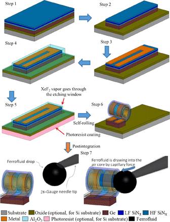
Illustration of the fabrication process flow for an air-core S-RuM inductor including the vapor phase releasing and the postfabrication capillary core filling approach for strong magnetic induction.
Route to integrating a magnetic core into monolithic 3D coils
S-RuM 3D microtube architectures inherently provide a cylindrical cavity for ferrofluid integration, a natural geometrical advantage unavailable to conventional planar processing. Ferrofluids were successfully incorporated in energy harvesters and actuators (31, 32); however, the methods used in these devices were beyond the domain of microelectronics fabrication, both in dimension and compatibility. For S-RuM 3D coil core-filling in this work, ferrofluid composed of nanoscale ferromagnetic, or ferrimagnetic, particles suspended in a carrier fluid (usually an organic solvent) was used. It is known that superparamagnetic nanoparticle suspension can be directly injected by fine-point syringes or transferred by a probe tip, taking advantage of the surface tension of the liquid dispersant. Capillary action directly aids liquid injection into a microtube by drawing ferrofluid introduced at the open end of the S-RuM microtube toward the center, enabling a high fill factor naturally. Suitable ferrofluids must have an appropriate surface tension and viscosity to be drawn into the air core by capillary forces at the desired speed. Uniformity, stability, and mass density are the primary requirements for the dispersion of nanoparticles in the liquid carrier.
Step 7 of Fig. 1 shows the three-step postfabrication core-filling process involving iron oxide nanoparticles as the magnetic material for an S-RuM Cu 3D coil air-core inductor. The three steps of this process are aligning, filling, and detaching. The tip of the micropipette (black shadow on the left) is first aligned with the S-RuM 3D coils. Then, one end of the S-RuM power inductor is attached to the ferrofluid droplet dangling from the tip of the micropipette. Core filling is triggered by the strong capillary interaction between the liquid carrier droplet and the microscale tubular air-core structure, and the result is the delivery of ferrofluid into the core of the inductor in a few seconds (movies S1 and S2). After the core is fully filled, the tip of the micropipette is retracted and detached from the end of the S-RuM 3D coils as shown, and the ferrofluid-filled tubular structure is left to dry. The core of an S-RuM 3D coil can also be filled multiple times after successive drying steps to evaporate the dispersant (cf. core-filling method in section S3). The core-filling process requires only that a micropipette, the ferrofluid delivery tool, has an exit diameter close to that of the S-RuM structure(s), resulting in a process that is simple, fast, clean, controllable, and reversible.
Underlying mechanics and general design approach
Experimental results and computational modeling suggest that the design of 3D S-RuM architectures for strong magnetic induction requires comprehensive mechanical/electrical/thermal management for predictable and optimized performance. Finite element analyses throughout every aspect of design provide context for general, rule-based procedures for obtaining magnetic induction systems with the desired performance. Consequently, these analyses have been found to be an essential element of the design process for practical applications. As shown in Fig. 1, the structural design of S-RuM 3D coils includes the vertical layer construction of layers and the horizontal layout before rolling. The coil inner diameter, the key parameter throughout the design process, is dictated by the properties and thicknesses of the material layers adopted for the vertical construction design. Given these data, a quasi-dynamic finite element method (FEM) is then used to accurately predict the value of the inner diameter based on the vertical construction of the layers (19). Figure 2A shows a simulated rolled-up membrane structure comprising a layered material stack as indicated, with an inner diameter of 140 μm. Figure 2B shows the tilted and side view (inset) scanning electron microscopy (SEM) images of the corresponding fabricated device, demonstrating agreement between the experimental and simulated values. The results of Fig. 2 (A and B) are representative of those obtained throughout these studies, thus providing support for the reliability of the quasi-dynamic FEM (details of the modeling can be found in section S4).
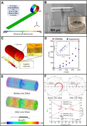
(A) FEM quasi-dynamic model for the rolling progress of stacked layer membrane with the thickness of each layer and the inner diameter labeled. (B) SEM image of the fabricated 14-turn S-RuM structure in (A) with the measured inner diameter labeled. (C) FEM electrical-thermal model built in COMSOL for the estimation of the temperature profile of a 12-turn Cu S-RuM structure with input DC current of 175 mA. (D) Comparison between the modeled and the measured data of the maximum temperature and structure resistance rise versus input DC current for the S-RuM structure in (C). (E) FEM electromagnetic model for calculating the S parameters of the S-RuM structure and the intensity of the magnetic induction inside the core before and after the core is filled at 10 MHz. Electrical properties of the structure with 0.813-W input power are measured and then used in the simulation. (F) Comparison between the simulated and the measured S11 of the structure in (E) and the calculated relative permeability and ferromagnetic resonance (FMR) resistance of the ferrofluid material at LF in two different structures.
The strength of magnetic induction for the microcoil technology described here clearly depends on their current handling ability. However, increasing current also raises the level of Joule heating, and the magnitude of the temperature rise depends primarily on the out-of-plane structural details. The physical dimensions of the rolled-up coil structure, such as the inner diameter and width of the metal strip and the layered structure design, play crucial roles in determining the rate at which temperature rises with increasing current. Joule heating in the copper strips was simulated using COMSOL by applying a range of currents from 100 to 225 mA (details of the model can be found in section S5). Shown in Fig. 2C is the modeled electrical-thermal profile of a representative S-RuM 3D coil architecture sitting on a sapphire substrate at an input current of 175 mA. As can be seen, there is a temperature distribution along the axial direction, with the uppermost sections of the inductor (furthest from the substrate) being the hottest, whereas the temperature distribution is uniform across the entire tube length. Figure 2D plots the modeled maximum temperature rise (taken along the dotted line at the top surface of the tube inductor in Fig. 2C) together with the experimental value from infrared (IR) measurements, as a function of input current in the range of 50 to 250 mA. The modeled and the experimental data do show a similar trend, i.e., increasing temperature rise with increasing current, but the modeled values clearly overestimate the temperature rise, and the discrepancy becomes larger at higher input current level. However, as shown in the inset of Fig. 2D, the match is excellent between the measured DC resistance of the 3D coil as a function of input current and the estimated values from the simulation. This validates the modeled Joule heating contribution because the rise in resistance with current can be attributed to the self-heating within the 3D coil at these current values (100 to 225 mA) and the positive temperature coefficient of resistance of copper. The overall thermal transport model from COMSOL needs to be refined to have an accurate estimation of all the thermal dissipation mechanism of the material system of S-RuM architecture, including thermal radiation, air convection, etc. Nonetheless, the model helps guide the thermal design of the S-RuM 3D coil architecture under a wide range of biasing conditions, along with input from IR temperature measurements for various structures.
Once the structural dimension and current handling ability are determined, the strength of magnetic induction can then be estimated by the FEM electromagnetic modeling for S-RuM 3D coil architectures. Because the metal strips used in the present S-RuM coil designs are much wider than the previously reported S-RuM radio frequency (RF) devices, the skin effect must be taken into consideration in the electromagnetic (EM) simulation to better describe the dependence of the resistivity on frequency, especially at HF. We note that for spherical Fe3O4 nanoparticles (d ≈ 10 nm) dispersed in a fluid, superparamagnetic behavior emerges, which is distinctly advantageous in HF applications because the single domain nanoparticle magnetic moments of the single-domain nanoparticles reorient more rapidly than their ferromagnetic counterparts because of Néel relaxation and Brownian motion. Furthermore, the nanoparticles require a magnetic field of lower magnitude to be applied for magnetization, and they do not suffer from the same losses as thin-film magnetic materials (33–35). Because detailed analytical or FEM modeling of the magnetic behavior of ferrofluids is problematic, in this work, the relationship between important ferrofluid material properties [energy loss due to the ferromagnetic resonance (FMR) and permeability] and frequency is first derived from the measured S parameters of a given ferrofluid material, and those for the ferrofluid loaded into a S-RuM coil with known geometry and dimensions. A model based on the experimentally established relationship is then integrated into the FEM S-RuM coil EM model to predict the performance of other designs (see details in section S6). Figure 2E shows the modeled magnetic flux density distribution of a representative two-cell three-turn S-RuM structure with an inner diameter of 140 μm both with and without the ferrofluid core, respectively. The maximum intensity of the magnetic induction inside the tubular structure is simulated accordingly with an input signal power of 0.813 W at 10 MHz with DC resistance of 7.7 ohms, which only increases the maximum operating temperature of the structure by 40°C (see details in section S7). The calculations show a maximum magnetic induction of 0.873 mT with air core and 1.9× improvement of the relative permeability with ferrofluid core. Figure 2F shows the corresponding raw S11 parameter between the modeled and the measured data in the Smith chart up to a frequency of 20 GHz and 500 MHz with the air-core and ferrofluid-core devices, respectively. In addition, the variation of the relative permeability and the FMR energy loss of the inductors with frequency are shown for two ferrofluid structures. The latter is represented as a resistance, and the results are given in a frequency range of 30 to 100 MHz where the cross-talk capacitance (19) between turns can be ignored. Structure 1 is the two-cell three-turn structure shown in Fig. 2E and the upper figure in Fig. 2F. Structure 2 is a four-cell 14-turn structure that has a larger volume to store ferrofluid. Moreover, structure 2 was filled three times, with time in between to dry the ferrofluid. As a result, structure 2 shows ~2× improvement of the relative permeability of the core material, as shown in the lower figure in Fig. 2F, indicating that multifilling effectively increases the volume of the magnetic nanoparticles. However, the FMR resistance of structure 2 is much larger than that of structure 1, which can be attributed to the more serious interparticle interaction loss (e.g., collision and friction) in the aggregated polydomain magnetic material.
Representative S-RuM 3D strong magnetic induction devices
DC/DC power converters are widely used in Internet of Things and cyber-physical system units to regulate the input levels of the voltage supply from a few volts to tens of volts. Following Moore’s law, the transistor node has been scaling down toward 3 nm, resulting in highly integrated logic control circuit; however, the bulky power inductors still dominate the overall size of power converters because of the extreme difficulty in scalability. The key specification requirements in the design and fabrication of compact power converters become more stringent. On the other hand, the switching frequency of emerging power converters has been pushed to as high as tens to hundreds of megahertz, which substantially reduces the inductance requirements down to tens to hundreds of nanohenries. Whether the power system in packaging (PSiP) or on-chip (PSoC) approach is used for power inductor design and fabrication, the planar spiral structure has almost always been the single best choice because of the prerequisite compatibility with planar semiconductor processing technologies. However, low inductance density and serious substrate parasitic effects, such as eddy current and parasitic capacitance effects associated with the planar design and fabrication regime, inherently limit the inductance density and the switching frequency.
With the S-RuM strong magnetic induction schemes outlined above, S-RuM power inductors with diverse geometry parameters and wide-ranging electrical performance can be realized in many different 2D layout designs using a variety of core materials. Here, we present five batches of S-RuM power inductors with Cu thicknesses of 150 to 225 nm and different numbers of cells, and each cell has the same width of 250 μm but different lengths scaled from 0.8 to 10 mm. Summarized in Fig. 3A is the length comparison of all batches before rolling with the scale indicated on the left y axis. The corresponding side-view SEM images of fully rolled-up batch 1, 2, and 4 devices, with the number of turns indicated, are shown on the right side. The most number of turns is obtained from the batch 5 design, which is ~23 turns with an inner diameter of ~140 μm with the total rolling length of each Cu strip of 1 cm.

(A) The planar layout of six batches of successfully fabricated devices with the total rolling length (0.8 to 10 mm) and rolling direction, as well as the number of cells indicated. SEM images show the cross sections of the fully rolled-up devices from batches 1, 4, and 5, with the number of turns indicated. (B to D) Ferromagnetic fluid drawn into a micropipette by capillary action with a droplet hanging at the tip (B); the pipette tip makes contact with the S-RuM air-core inductor tube (B), and capillary action forces the ferrofluid into the core of the inductor tube (C). Then, the pipette was withdrawn and detached from the core-filled S-RuM inductor tube (D). (E) Optical images of a six-cell 21-turn inductor before and after core filling. (F) A single two-cell inductor sitting on a piece of sapphire substrate placed by a U.S. penny for size comparison. (G) Optical image of an array of S-RuM inductor tubes fabricated monolithically.
A critical enabler of the scaling scheme to increase the number of turns, by rolling-up centimeter and beyond long strips, is to use XeF2 dry etch to release the Ge sacrificial layer instead of using wet etching solutions. The dry etching releasing method produces a rolling speed of ~750 μm/min (movies S3 and S4), which is over 500 times faster compared with any wet etching methods previously reported (28). The fast rate provides the rolling momentum for a much heavier load such as Cu strips with hundreds of nanometers in thickness, hundreds of micrometers in width, and centimeters in length. In addition, the superfast dry releasing speed bypasses the overwhelming pinhole issues that used to trigger detouring and failure during the rolling progress even when the rolling length was under 1 mm long.
Figure 3 (B to D) demonstrates the three-step core-filling process. First, the ferromagnetic fluid is drawn into a 28-gauge micropipette by capillary action, with a droplet hanging onto the tip of the pipette. Second, the pipette is lowered until it is nearly leveled with the inductor tube and is moved toward the tube to make contact. Last, once the contact is made between the inductor and the micropipette, the ferrofluid inside the pipette is drawn into the inductor tube, which has an even smaller diameter, by capillary action. Figure 3E shows an optical image of a six-cell, 21-turn inductor before and after being core-filled with the ferromagnetic fluid. For visual purpose, a single inductor device sitting on a piece of sapphire wafer was cut off from the rest of the inductor tubes in the array by a laser cutter and placed beside a U.S. penny for size comparison in Fig. 3F. A 3 × 3 array of fully fabricated and core-filled two-cell S-RuM inductor tubes is shown in Fig. 3G.
The measured frequency dependence of the inductance and the Q factor of all batches of devices without the core filled is shown in Fig. 4 (A and B) (see detailed structural dimension of all batches in section S8). Just as it was the case for S-RuM RF inductors reported previously (19, 28), inductance shows a superlinear relationship with the number of turns. The batch 5.2 device has an inductance as large as 140 nH at 10 MHz, a maximum working frequency at 2 GHz, and a maximum Q factor of 2.3 at 250 MHz. Compared with the batch 1 device, the inductance per cell is improved by 46.7× by increasing the length of the Cu strip by 12.5×. The resonance frequency continues to drop from batch 1 (>20 GHz) to batch 5.2 (>1.3 GHz), but with rapidly decreasing rate because of the weakened influence of cross-talk coupling capacitance between turns (19). This implies that, unlike the planar counterparts, the operating frequency of S-RuM power inductors can still be high even when larger inductance is obtained. The maximum Q factor at 250 MHz is ~2.85, improved by 11.4× from the previously reported best result of ~0.25 (30), because vapor-phase releasing enabled large cross-sectional area Cu strip rolling. Once the air core is filled by ferrofluid, the operating frequency drops because of the FMR of the available iron oxide nanoparticles used for this study. To better study the performance of S-RuM power inductors at ultralow frequency below 10 MHz, the data collected from Keithley Clarius and Copper Mountain Technologies vector network analyzer (CMT VNA) are combined to show the relationship between the inductance and the Q factor versus frequency (Fig. 4C). It can be seen that the inductance reaches 1.24 μH at 10 KHz, and the maximum Q factor is 0.9 at 10 MHz for the batch 5.2 device. The corresponding inductance area and volume density are 3 μH/mm2 and 23 μH/mm3, respectively. Compared with the air-core devices, the maximum inductance and Q factor enhancement due to ferrofluid core filling at LF are ~9× and 3×, respectively. The improvement of the Q factor is not as much as that of inductance because of the FMR loss. To examine whether the air core is filled by the ferrofluid to the limit, the batch 4.2 device was filled and measured three times. Slight improvement was shown after the second filling, but nearly the same inductance (and Q factor) versus frequency was found between the second and third rounds of filling, as shown in Fig. 4 (C and D), indicating that two-time core filling is sufficient for this case. Figure 4E shows the resonant frequency of the batch 4.2 and 5.2 devices, which are both above 500 MHz. Compared with the bulk iron oxide material, monodomain iron oxide nanoparticle has much large FMR frequency, implying an important application when high power and HF are both required. Figure 4F benchmarks the inductance area density versus the operating frequency, plotted on a double log scale, of the S-RuM power inductor devices against state-of-the-art planar counterparts from literature as cited. Clearly, the S-RuM devices show much higher inductance density across the entire frequency range. Furthermore, they demonstrate unique capability in HF operation, which fits the need of the next generation of power device with a switching frequency range of 100 to 500 MHz. The S-RuM power inductor performance can be further improved by scaling the rolling length of the metal strips longer, wider, and with better conductivity.

(A and B) Inductance (solid line) and Q (dashed line) versus frequency of air-core devices from batches as indicated from 10 MHz to 20 GHz (A) and 10 MHz to 3 GHz (B). (C and D) Inductance (C) and Q factor (D) versus frequency of ferrofluid-core devices from batches 4.2, 5.1, and 5.2 at frequency below 10 MHz measured using Keithley Clarius (10 KHz to 4 MHz, solid line) and CMT VNA (2 MHz to 10 MHz, dashed line). (E) Inductance (solid line) and Q factor (dashed line) versus frequency of ferrofluid-core devices from batches 4.2 and 5.2. at frequency above 10 MHz up to resonance frequency. (F) Inductance density versus frequency performance comparison between S-RuM power inductors and other state-of-the-art planar counterparts with/without magnetic core (36–40). (G) Left: Measured thermal image of a batch 4 air-core device with an input current of 250 mA. Right: Temperature distribution line scan along the black line drawn across the inductor tube in the image under different input DC current as indicated.
Current handling ability is determined by measuring the thermal profile along the axial direction on top of the device using an IR thermometer. Shown in Fig. 4G is the thermal map of a batch 4 air-core device. The background temperature was set to 50°C to obtain a reasonable signal-to-noise ratio. The input current was set to 250 mA with measured maximum temperature of ~400°C without destroying the device (see details in section S7). This indicates that the maximum power the batch 4 S-RuM power inductor can handle is at least 0.94 W, with corresponding power density of ~8.5 W/mm2 and a simulated maximum magnetic induction of 12 mT in the core at 10 MHz.
On the basis of the above representative demonstration, it is clear that the S-RuM architecture is unique in that it enables the concentration of a magnetic field through the center axis of a hollow cavity, which can support a fluid and confine it through capillary action. This feature allows the integration of a unique class of core materials, ferrofluids, which can be optimized for higher frequencies than what is possible with planar-deposited magnetic alloys. Theoretically, the thermal conductivity of the oil-based ferrofluid is much larger than that of air, which implies a positive impact on helping distributing the Joule heating.
DISCUSSION
We have reported an efficient 3D magnetic energy storage architecture based on a monolithic strain-induced multiturn S-RuM platform combined with postfabrication capillary core filling for mtesla-level magnetic induction. The structural design, fabrication process, and multiphysics modeling have been systematically studied to demonstrate the capability of obtaining microhenry-level inductance with inductance density as large as tens of μH/mm3 and maximum operating frequency of hundreds of megahertz, with at least 12-mT magnetic induction inside the core. In contrast to planar architectures, the S-RuM architecture offers a third dimension in design and a simple and efficient way to integrate high-performance magnetic materials. This ensures a much larger magnetic flux density both inside or surrounding the 3D structure. Furthermore, the monodomain magnetic nanoparticles in the ferrofluid have much smaller FMR frequency compared with bulk material, which enables strong magnetic induction even at HF. With improved ferrofluid material, a better way to dissipate generated heat, and appropriate apparatus to precisely control the ferrofluid core filling, the magnetic induction could be as large as hundreds to thousands of mtesla and be reconfigurable because of the fluidic nature of the core material. The fabrication process of air-core S-RuM architectures is fully compatible with all planar semiconductor processing including CMOS (complementary metal-oxide semiconductor) and MEMS technologies, and it is also low in cost due to the simple fabrication requirement of three-step optical lithography, without any special substrate treatment, in addition to the small on-chip footprint. The core-filling technique demonstrated can be made compatible with back-end-of-line (BEOL) wafer fabrication if the fluid transporting and dispensing are automated by using an array of robotic needles instead of a single manual micropipette demonstrated here. Manufacturing challenges, including encapsulation of the ferrofluid core–filled tubular devices, will also need to be addressed before practical integration of this device with the current state-of-the-art high–magnetic induction devices. Successful demonstration of power inductors using the S-RuM architecture paves the way for the broader applicability of this platform. As the integration technology for ferrofluids into modern microelectronics matures, the feasibility to integrate more highly engineered fluids into a broader class of electromagnetic devices such as energy harvesters and cooling apparatuses will benefit their performance and unlock new levels of integration with silicon and biological systems, among others.
MATERIALS AND METHODS
Ferrofluid material
EMG 900 oil-based ferrofluid from Ferrotec was used in experiment. The carrier solution was a light hydrocarbon oil, and the diameters of ferromagnetic nanoparticles fit a distribution centered at 10 nm as shown in fig. S2. In EMG 900, ferromagnetic nanoparticles occupy 17.7% of the ferrofluid in volume, which is the highest commercially available ferrofluid to our knowledge.
Fabrication method of S-RuM architectures
A C-plane (0001) sapphire wafer was used as the substrate, followed by electron beam (E-beam) evaporation to deposit 100-nm-thick germanium (Ge) film as the sacrificial layer because of the smooth surface and the relatively large Young’s modulus for avoiding surface roughness accumulation and strain sharing. Next, a 5-nm-thick Al2O3 thin-film layer was deposited by ALD to protect the Ge sacrificial layer. Considering planar processing compatibility, a low-temperature PECVD was used to grow the strained “rolling vehicle,” which included a 20-nm-thick LF (~−1168 MPa compressively strained, 360 kHz) silicon nitride (SiNx) layer and a 20-nm-thick HF (~406.95 MPa tensile-strained, 13.56 MHz) SiNx layer deposited in sequence. Freon reactive ion etching was then used to etch the layer stack to reach the surface of the sapphire wafer to form a mesa. Afterward, the Cu metal layer was deposited by E-beam evaporation, followed by photolithography patterning to form coil strips. The metal layer was a bilayer structure, which consisted of a 5-nm Ni underneath the major highly conductive Cu metal with thickness up to 180 nm, where the Ni thin film was used as an adhesion and a nucleation layer as well as an oxidation prevention layer for achieving high conductivity of metal thin film. Next, 20-nm-thick Al2O3 thin-film layer was deposited by ALD, which serves as a cover layer together with the 5-nm Al2O3 thin-film layer on top of the Ge layer to avoid any oxidation of the conductive metal and protect the sacrificial layer from unwanted wet etching due to inherent pinhole issues within the SiNx bilayer. A window was then opened down to the substrate at the long end of the mesa opposite to the contacts. Upon etching the Ge sacrificial layer by XeF2 vapor, the Cu strips automatically self-assembled by directional rolling into multiturn hollow tubular structure. More detailed processing parameters can be found in section S1.
Capillary core-filling method
We prepared a 28-gauge, 67-mm-long MicroFil micropipette (plastic + fused silica) and attached it into a micromanipulator for directional control as shown in fig. S2 (C and D). Next, we drew ferrofluid into the micropipette from the dish container by capillary action. We lowered the micropipette tip under the microscope until it touched the surface near the tube. The tip of the micropipette was then aligned with the S-RuM structure. We moved one end of the S-RuM structure to attach the ferrofluid hanging on the tip of the micropipette, and the core filling was triggered using strong capillary force between large–surface tension liquid carrier and microscale-diameter tubular structure to deliver ferrofluid into the air core. After the core was fully filled, the tip of the micropipette was detached from the end of the S-RuM structure.
AC/DC characterization of S-RuM architecture
The tools used to measure the inductance of batch 4 and 5 power inductors were a CMT VNA and a Keithley 4200A-SCS Parameter analyzer. Measuring the inductor’s inductance through the VNA at the mid-frequency to the HF range relies on measurements via scattering parameters (S parameters), which are valid in the frequency range where the wavelength of the measurement frequency is large compared with the physical dimensions of the device, and the device must be considered as a distributed electrical network. However, in the kilohertz and low-megahertz range, VNAs typically cannot measure S parameters accurately because of the need to couple the measurement signal into a highly resistive waveguide coupler. For waves in the kilohertz frequency range, the coupling coefficient of this system is low, and the measurement becomes inaccurate. It is also prohibitively difficult to measure voltage and current simultaneously at high frequencies to extract a reactance metric through a direct measurement of impedance. To obtain a more accurate inductance data in the kilohertz to the low-megahertz range, the Keithley instrument was used to measure the value of the complex impedance of the inductors. The lower-frequency Keithley tool relies on measurements of voltage and current to extract an impedance metric, which is not possible at higher frequencies where S parameters must be used. Plot in Fig. 4C includes both measurements in an attempt to show the overlap of inductance in the low-megahertz range, where the CMT VNA starts to measure more accurately than the Keithley parameter analyzer as frequency increases. It is impossible to define a cutoff frequency where one tool and measurement method becomes more accurate than the other, even considering the specifications of the tool manufacturer, so both measurements over the overlapping frequency range are shown for transparency. Plot Fig. 4D mirrors Fig. 4C to provide the Q factor of the same sets of inductors. We considered the “open-thru” de-embedding of any parasitic parameters such as contact resistance, and the parasitic inductance and capacitance from the testing fixture over the operating frequency band. Two-port S parameters were measured by using the Agilent PNA8363C performance network analyzer with Cascade Microtech air coplanar ground-signal-ground probes in the frequency range from 10 MHz to 18 GHz (see details in section S9). The DC square resistance was obtained from the two-probe measurement. The resistance of the two probes shorted together was first measured and then subtracted from the measurement data.
Thermal characterization of S-RuM architecture
To experimentally measure the self-heating in these rolled S-RuM architecture, we used IR thermometry to map the temperature profiles of the devices under applied electrical bias. We wirebonded the rolled inductor contact pads to larger copper pads for probing and then applied currents ranging from 30 to 250 mA with a Keithley 2612 SourceMeter. For the IR measurements, we used a Quantum Focus Instruments InfraScope with an indium-antimonide IR detector cooled using liquid nitrogen. The stage temperature was slightly elevated with respect to ambient and was set to 50°C to improve the signal-to-noise ratio. An optical image of the wirebonded device is shown in fig. S10A, with the corresponding IR image in fig. S10B when 225 mA was applied through the device.
SUPPLEMENTARY MATERIALS
Supplementary material for this article is available at http://advances.sciencemag.org/cgi/content/full/6/3/eaay4508/DC1
Section S1. Detailed fabrication flow
Section S2. The “round corner” design of Cu strip
Section S3. Detailed core-filling method
Section S4. Detailed mechanical FEM for inner diameter estimation
Section S5. Electrothermal modeling of S-RuM architecture
Section S6. Electromagnetic FEM modeling of S-RuM architecture
Section S7. IR imaging of S-RuM architecture
Section S8. Structural dimension of all S-RuM power inductor samples
Section S9. HF measurement details of S-RuM power inductors
Fig. S1. Mask-level depiction of the planar inductors.
Fig. S2. Capillary core-filling material and method for S-RuM architecture.
Fig. S3. Electrical-thermal modeling of S-RuM architectures.
Fig. S4. Electromagnetic FEM modeling of S-RuM architecture skin effect.
Fig. S5. LF (<~100 MHz) equivalent circuit of S-RuM architecture with ferrofluid core with enhanced inductance and introduced additional loss from FMR represented as LFL and RFMR, respectively.
Fig. S6. The complete FEM model in HFSS to simulate the S parameters and the intensity of magnetic induction in the core of the S-RuM architecture.
Fig. S7. IR imaging of S-RuM architectures.
Fig. S8. Temperature profiles measured across the white dotted line of the exemplary structure shown in Fig. 2E (also the batch 2 device) with DC current of 325 mA.
Fig. S9. Open-through de-embedding patterns and their corresponding lumped equivalent circuits.
Fig. S10. Mathematical procedure to do the open-through de-embedding.
Table S1. Material property set in FEM modeling simulation.
Table S2. Parameters for COMSOL simulations.
Table S3. Primary dimensional parameters of all batches.
Movie S1. Ferrofluid filled into a short S-RuM architecture.
Movie S2. Ferrofluid filled into a long S-RuM architecture.
Movie S3. The rolling progress of a 1-cm-long S-RuM architecture observed with 10× real speed.
Movie S4. The rolling progress of 1.6-mm-long S-RuM architecture array observed with 10× real speed.
This is an open-access article distributed under the terms of the Creative Commons Attribution-NonCommercial license, which permits use, distribution, and reproduction in any medium, so long as the resultant use is not for commercial advantage and provided the original work is properly cited.
REFERENCES AND NOTES
- ↵
- ↵
- ↵
- ↵
- ↵
- ↵
- ↵
- ↵
- ↵
- ↵
- ↵
- ↵
- ↵
- ↵
- ↵
- ↵
- ↵
- ↵
- ↵
- ↵
W. Huang, J. Zhou, P. Froeter, K. Walsh, S. Liu, J. Michaels, M. Li, S. Gong, X. Li, CMOS-compatible on-chip self-rolled-up inductors for RF/mm-wave applications, paper presented in the 2017 IEEE MTT-S International Microwave Symposium (IMS), Honolulu, HI, 4 to 9 June 2017.
- ↵
- ↵
- ↵
- ↵
- ↵
- ↵
Acknowledgments: Funding: This work was supported, in part, by the National Science Foundation Engineering Research Center for Power Optimization of Electro-Thermal Systems (POETS) under Awards EEC no. 1449548 (W.H., Z.Y., J.M., X.L., P.V.B., E.P., and D.S.) and IIP no. 17-01047 (M.D.K., Q.W., and X.L.); the U.S. Department of Energy (DOE), Office of Science, Basic Energy Sciences (BES) under award no. DEFG02-07ER46471 (W.H., S.L., X.L., P.V.B., and Q.C.); and the National Natural Science Foundation of China under award no. 61974038 (W.H.). Author contributions: X.L. designed and supervised the research. W.H. led the structural designs, mechanical modeling, and electromagnetic modeling, with assistance from H.Y. and L.S. W.H., Z.Y., and M.D.K. led the fabrication of all samples, with assistance from Q.W. and S.L. W.H. and Z.Y. led the DC and RF electrical measurement, with assistance from M.D.K., D.J.S., and S.G. W.H., J.H.N., and Z.Y. led and designed the capillary core filling method, with assistance from Z.O. and M.D.K. A.S.Y. led the electrical-thermal modeling, with assistance from M.M.R. and W.H. M.M.R. led the IR measurement, with assistance from F.L., V.C., and W.H. All authors commented on the paper. Competing interests: X.L. and W.H. are inventors on Patent 15/704,262 (26 November 2019) that covers rolled-up power inductor and array of rolled-up power inductors for on-chip applications. X.L., W.H., J.H.N., J.G.E., Z.O., and Q.C. are inventors on pending Patent 62/682,569 (7 June 2019) that covers rolled-up magnetic component for on-chip applications and method of making a rolled-up magnetic component, all submitted by the University of Illinois at Urbana-Champaign. F.L. is currently affiliated with Northrop Grumman Aerospace Systems, Redondo Beach, CA 90278, USA. J.H.N. is currently affiliated with CCDC U.S. Army Research Laboratory, Sensors and Electron Devices Directorate, Electro-Optics and Photonics Division, Adelphi, MD 20783, USA. X.L. is also affiliated with the Materials Research Laboratory, the Department of Mechanical Science and Engineering, the Beckman Institute for Advanced Science and Technology, University of Illinois at Urbana-Champaign. Data and materials availability: All data needed to evaluate the conclusions in the paper are present in the paper and/or the Supplementary Materials. Additional data related to this paper may be requested from the authors.
- Copyright © 2020 The Authors, some rights reserved; exclusive licensee American Association for the Advancement of Science. No claim to original U.S. Government Works. Distributed under a Creative Commons Attribution NonCommercial License 4.0 (CC BY-NC).


